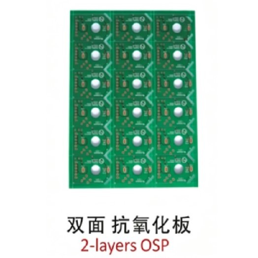
2-Layer High Frequency PCB for Antenna | OSP Finish | Low Loss
Product Overview:
This high-performance 2-layer High Frequency PCB is specifically engineered for advanced antenna applications. Utilizing premium low-loss materials and high-stability FR4 substrates, it ensures exceptional signal integrity for RF and microwave communications. The OSP (Organic Solderability Preservatives) surface finish provides a flat, reliable soldering surface while maintaining optimal electrical performance. Perfect for wireless modules, radar systems, and IoT devices.
Key Selling Points:
• Superior Signal Integrity: Optimized for RF & antenna high-frequency transmission.
• Low Insertion Loss: Premium materials minimize signal attenuation and heat.
• OSP Surface Finish: Ensures excellent flatness and reliable component assembly.
• Custom Design: Fully tailored to your specific antenna impedance requirements.

Engineering Support: DFM (Design for Manufacturing) check before production.

Testing: Flying Probe Test, Fixture Test, Impedance Control Test, Thermal Stress Test.
“ Instant PCB(1-38 layers)”--PCBgate
PCBgate is a professional PCB manufacturer providing high-quality printed circuit boards for global electronics industries.
We are capable of manufacturing a wide range of PCB types to meet different application requirements, including:FR-4 PCBs,ceramic PCBs,carbon oil PCBs,Aluminum PCBs,Flexible & Rigid-Flex PCBs.

We specialize in High-Frequency PCB manufacturing for advanced antenna systems, providing the perfect balance between signal integrity and thermal stability. By utilizing precision impedance control and advanced vacuum etching, we achieve the consistent dielectric performance and low-loss transmission required for RF and microwave designs.
This 2-layer structure with OSP finish is ideal for 5G telecommunications, automotive radar, and satellite navigation. We ensure rigorous E-test and signal integrity inspection to guarantee that every antenna board meets the highest industrial standards for high-speed performance.
We support High-Frequency PCB prototypes, small-batch production, and mass production to meet different customer requirements, offering expertise in handling premium materials like Rogers and Arlon.
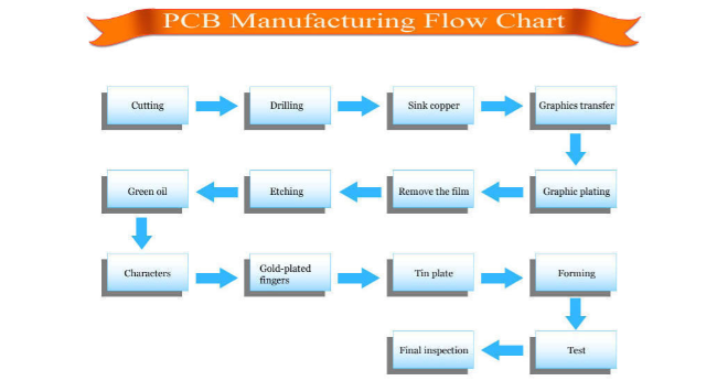
Our PCB manufacturing capability includes:
• Premium RF Materials: Rogers, Arlon, and Teflon
• Hybrid Lamination: FR-4 + High-Frequency material hybrid stack-ups
• Low-Loss Performance: Low Df materials for minimal signal attenuation
• Surface Finishes for RF: Immersion Silver, ENIG, and ENEPIG for optimal conductivity
• High-Layer RF Structures: Multilayer high-frequency boards up to 20+ layers
• Quick-Turn Service: Rapid prototyping for RF and Microwave designs

Attention: pictures are for reference only. The specific products are subject to the original factory model.


Standard Packaging: Inner Vacuum Packaging + Outer Carbon Box.
Delivery Partners: EMS,DHL,SF-express, FedEx, UPS or Sea/Air Freight for bulk orders.

• 15 years of experience in PCB manufacturing.
• Advanced Equipment: Equipped with high-speed CNC drilling machines and AOI testing lines.
• Professional engineering support
• Fast prototype delivery
• Global customers from Europe, USA and Asia
• Own Global Supply System.
• Fast and safe way by EMS/DHL/SF-express/Fedex,etc.
• New styles updating everyday and MOQ for all the styles;

1. What's your MOQ and what is PCBgate's fastest delivery time?
A: Our MOQ is Minimum packaging quantity, please contact us for details. Sample to mass production all can be supported by PCBgate.
2. Which payment terms does PCBgate accept?
A:Advance T/T,Western Union,Paypal, L/C,Credit Card, Cheque,Money Gram and Others.
3.What files are required for PCB quotation?
A:Gerber files, PCB specifications and quantity.
4. How to test PCB boards?
A: AOI, Fly probe testing, Text fixture testing, FOC etc. For bare PCB.
Shipping Information
| FOB Port Shenzhen |
Lead Time 7-15 days |
| Weight per Unit 1.0 Kilograms |
Dimensions per Unit 7.2x3.2x0.06 Centimeters |
| HTS Code 8517.79.90 00 |
Units per Export Carton 36.0 |
| Export Carton Dimensions L/W/H 58.0x26.0x36.0 Centimeters |
Export Carton Weight 0.1 Kilograms |
Welcome to send us your PCB Gerber files for quotation.
Our engineering team will respond within 24 hours.

|
|
2-Layer High Frequency PCB for Antenna | OSP Finish | Low Loss Images
|


